
Electroninks Launches CircuitJet IV PCB Manufacturing Platform
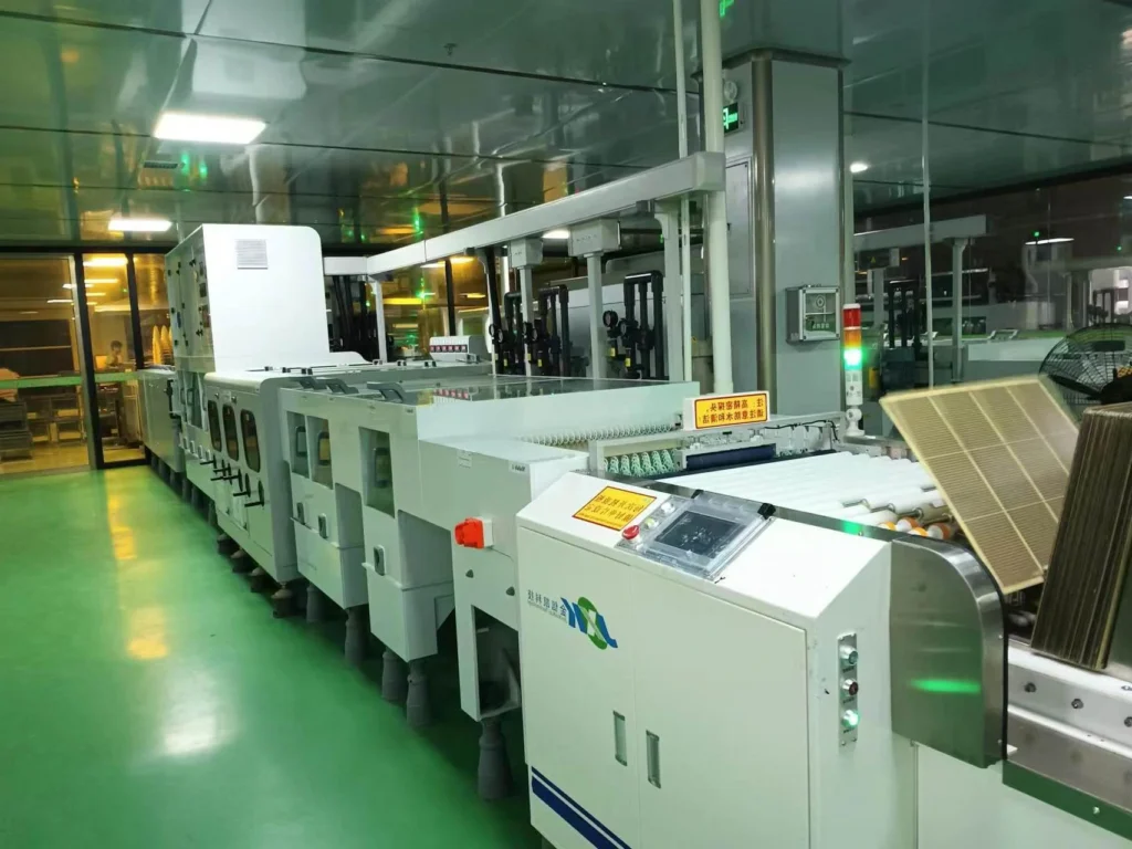
Electroninks has announced the launch of the CircuitJet IV, its latest platform for manufacturing printed circuit boards using additive inkjet technology. The system is designed to help engineers and product designers rapidly prototype and produce functional multi-layer PCBs without relying on traditional fabrication processes. Providing an in-house solution, the platform aims to shorten development cycles and lower entry barriers for electronics innovation.
Additive Manufacturing Meets PCB Fabrication
Conventional PCB production relies on subtractive techniques such as photolithography and chemical etching. These methods involve multiple processing steps, including material deposition, exposure, and development, followed by etching and stripping. Each stage introduces costs, material waste, and time delays. The CircuitJet IV replaces this workflow with a direct-write process that deposits conductive inks precisely where traces are needed.
By removing the need for photomasks and hazardous etchants, the platform simplifies production logistics. Changes to a board design can be implemented without altering hard tooling. This agility proves especially valuable during iterative design phases, when multiple revisions are common before a final layout is approved.
The approach aligns with broader trends toward sustainable manufacturing. Eliminating chemical etch baths reduces hazardous waste streams, and printing only the required amount of conductor reduces material consumption compared to full-panel copper lamination and etching.
Inside the CircuitJet IV Platform
At the core of the platform lies Electroninks’ expertise in particle-free conductive inks. Unlike conventional nanoparticle-based formulations, these solvent-based inks maintain stable jetting performance and deliver high conductivity upon curing. The absence of particles minimizes clogging in inkjet nozzles, enhancing reliability during prolonged print runs.
The system supports multi-layer construction by printing alternating layers of conductive traces and dielectric materials. Registration accuracy ensures alignment between layers, enabling complex circuit geometries. Flexible and rigid substrates are both compatible, allowing the machine to be used for a spectrum of applications ranging from flexible sensors to rigid IoT boards.
Operation is managed through intuitive software that converts standard PCB design files into print commands. This seamless workflow allows designers to move from computer-aided design to physical board in hours rather than days or weeks. The platform’s compact footprint also means it can fit into lab environments or small workshops, democratizing access to PCB prototyping.
Benefits for Rapid Prototyping
In-house PCB prototyping with the CircuitJet IV offers several strategic advantages. First, it dramatically reduces turnaround time. Instead of waiting for external fabrication houses, teams can iterate on designs within the same day. Shorter feedback loops lead to faster product development cycles and earlier market entry.
Second, the ability to keep early-stage designs confidential is enhanced. When sensitive board layouts are sent to third-party manufacturers, intellectual property risks increase. Producing prototypes on-site mitigates these concerns, especially for defense, medical, or other high-security applications.
Third, small batch production becomes economically viable. Low-volume runs that were once prohibitively expensive due to setup costs and minimum order quantities can be produced cost-effectively. This flexibility supports customized electronics, niche products, and research projects.
Finally, the platform fosters innovation by lowering the barrier to experimentation. Designers can test novel form factors and materials without committing to large investments in tooling, encouraging a more exploratory approach to electronics design.
Expanding the Electronics Manufacturing Toolkit
The introduction of the CircuitJet IV broadens the additive manufacturing toolkit for electronics, complementing established 3D printing technologies for structural components. Just as fused deposition modeling and stereolithography transformed mechanical prototyping, additive PCB fabrication promises to reshape how electronic systems are built.
Educational institutions and makerspaces stand to benefit significantly. Students can go from circuit theory to physical board in a single lab session, reinforcing learning through hands-on experience. Maker communities gain the ability to produce professional-grade PCBs without outsourcing, enabling sophisticated open-source hardware projects.
In the industrial sphere, maintenance and repair operations can leverage the technology to print replacement boards on demand. This reduces downtime for legacy equipment where original boards are no longer available. Field-service teams equipped with a portable printer could address critical failures without waiting for logistics support.
The platform also intersects with the growing interest in printed electronics beyond traditional PCBs. Conductive traces on unconventional substrates—such as textiles, paper, or biodegradable materials—open paths for wearable electronics, smart packaging, and transient devices. By enabling precise deposition of functional materials, the CircuitJet IV can serve as a development tool for these emerging categories.
A Step Toward Agile Electronics Development
The launch of the CircuitJet IV comes at a time when industries increasingly demand faster design cycles and greater customization. Whether for startups testing new concepts or large enterprises seeking to streamline R&D, the ability to produce boards internally with minimal overhead represents a meaningful shift.
While traditional PCB manufacturing will remain dominant for high-volume mass production, additive platforms are carving out a vital niche in prototyping, education, and specialty applications. As conductive ink formulations mature and print resolution improves, the gap between printed and etched boards continues to narrow.
The CircuitJet IV does not replace conventional fabrication lines but gives electronics developers a powerful new option. With this launch, Electroninks reinforces its position at the intersection of materials science and digital manufacturing, helping to bring integrated additive solutions to more workbenches around the world.
Why This Matters
This launch highlights the evolution of additive manufacturing into PCB fabrication, where traditional etch-based methods have long dominated. By enabling in-house, on-demand board production, such systems can shorten development timelines, reduce material waste, and make iterative electronics design more accessible across industries ranging from consumer wearables to industrial IoT.
FAQ
How does inkjet-based PCB fabrication differ from conventional etching?
Conventional PCB fabrication uses photolithography and chemical etching to remove copper from a substrate, leaving behind the desired traces. Inkjet printing, as used by the CircuitJet IV, deposits conductive ink directly onto the board material in a single additive step, eliminating the need for photomasks and chemical baths while reducing waste.
What types of substrates can the CircuitJet IV print on?
The platform is designed to handle both rigid materials like FR4 and flexible substrates such as polyimide films. This versatility makes it suitable for a range of applications, from standard circuit boards to flexible electronics and wearables.
Is the CircuitJet IV meant for mass production or prototyping?
The CircuitJet IV is optimized for rapid prototyping and low-volume production runs. While it can produce small batches cost-effectively, high-volume PCB fabrication still relies on traditional subtractive methods for economic efficiency at scale.
What role do Electroninks' conductive inks play in the system?
Electroninks developed particle-free silver inks that deliver high electrical conductivity and reliable jetting. These formulations are central to the CircuitJet IV's ability to create fine traces with consistent performance, avoiding the nozzle clogging issues common with particle-based inks.
Sources
Source: "PCB fabrication" – Google News